

Are There Any Downsides To Using One Register For All I/o In Pic
| | Previous Tutorial | Tutorial four | Next Tutorial | | |||
| Input/Output IO Ports – GPIO Pins | |||||||
| PIC Microcontrollers Course Home Page 🏠 | |||||||
in this tutorial, we'll address the Input/Output Ports in the Microchip PIC microcontrollers. You'll learn much nigh the digital input/output pins GPIOs in microcontrollers, how they piece of work and how to drive/interface them properly. We'll also flash some LEDs for testing out these concepts. With MPLAB ten IDE, XC8 Compiler, and PICKit2 or 3. There is besides a video guide by the terminate of this tutorial that you should bank check out.
Tutorial Contents
- one Required Components
- 2 What are GPIO pins?
- iii How does a digital input/output port work?
- iii.1 1. Configure i/o pins
- 3.2 two. Read/Write digital i/o pins
- 4 Flashing some LEDs – LAB
- 4.one i. Coding
- 4.two 2. Simulation
- 4.3 3. Prototyping
- 5 Reading Digital Inputs – LAB
- 5.1 1. Coding
- v.two 2. Simulation
- five.3 3. Prototyping
- 6 The power of #ascertain directive
- vii Checkout My PIC MCU Programming Video Tutorial
- eight Share this:
- 9 Like this:
- 10 Related
Required Components
| Qty. | Component Name | Buy On Amazon.com |
| i | PIC16F877A | Add |
| 1 | BreadBoard | Add |
| 3 | LEDs | Add Add |
| 2 | Push Buttons | Add |
| 1 | Resistors Kit | Add Add |
| 1 | Capacitors Kit | Add Add together |
| ane | Jumper Wires Pack | Add Add together |
| 1 | LM7805 Voltage Regulator (5v) | Add |
| 1 | Crystal Oscillator | Add |
| ane | PICkit2 or 3 Programmer | Add together |
| i | 9v Bombardment or DC Power Supply | Add together Add Add |
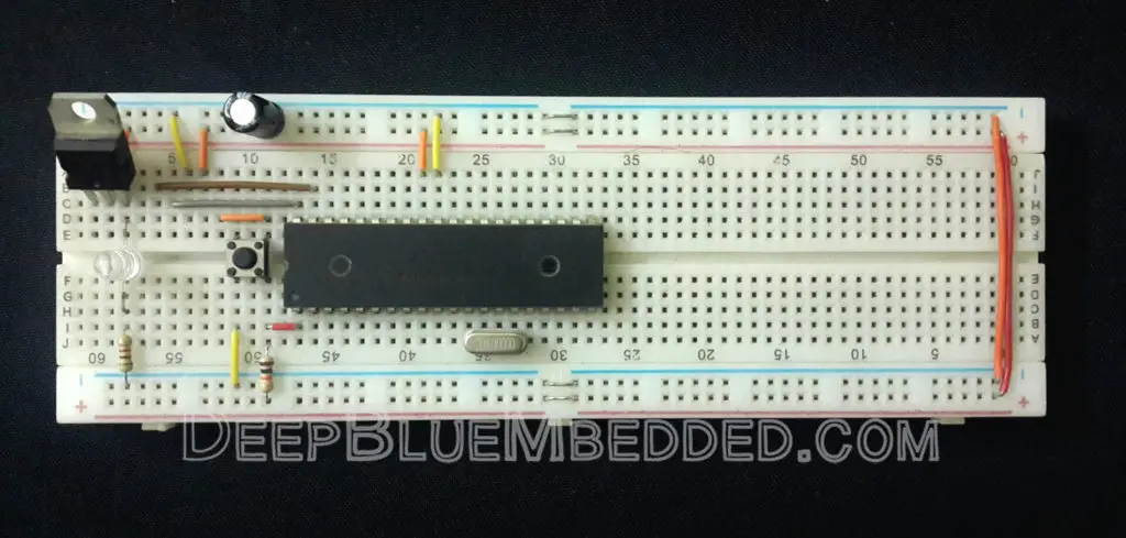
The Prototyping Board Setup
What are GPIO pins?
GPIO stands for "General Purpose Input/Output pins". In fact, almost of the pins in a typical microcontroller are GPIO pins except for some special pins. The special (non-GPIO) pins are unremarkably the post-obit ones:
- Power Supply pins: Vdd & Vss
- OSCillator pins: OSC1 & OSC2. Those couple of pins are used to provide the MCU with the oscillator clock input it needs.
- MCLR: the master clear reset pin. Used for restarting the MCU on purpose.
- VUSB: the external USB power source.
Except for the special office pins, all the other pins are GPIOs. As shown beneath from the PIC16F877A datasheet, the GPIO pins are clustered in PORTs.
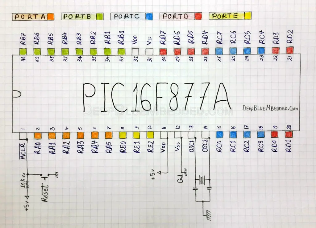
As y'all may have noticed that the pins [ii to 7] are named [RA0 to RA5] and that's why this is chosen "PORTA". In our MCU in that location are v digital Input/output ports [A, B, C, D, and Due east]. It'south mutual in 8-Bit microcontrollers to have I/O ports each of which has up to viii-pins. Nevertheless, some I/O ports may have less than 8-pins as in our PIC16F877A for examples. As you tin see
- PORTA: has six pins [2 to vii]
- PORTB: has 8 pins [33 to 40]
- PORTC: has viii pins
- PORTD: has viii pins
- PORTE: has 3 pins [eight to 10]
| Annotation | |||
| The pins of every unmarried port may not be in consecutive social club physically on the chip. Which is the case for PORTC & PORTD as you lot may have noticed | |||
How does a digital input/output port work?
Generally speaking, the I/O ports are operating similarly which mean that you but need to investigate ane of them. Then the other ones volition be using the exact same concept and working in a like manner. For this tutorial, nosotros'll exist using PORTB for our Demo. & Lab.
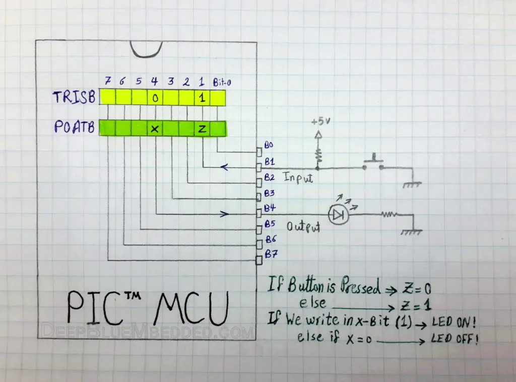
There are basically a couple of registers dedicated to each I/O port to command its performance.
- TRISx Annals
- PORTx Register
The registers dedicated to PORTA pins are (TRISA & PORTA), and the registers defended to PORTB pins are (TRISB & PORTB), so on.
Controlling or driving the I/O port is a pretty easy procedure. It involves only two sequent steps.
- Configure The Pin, determine the data direction, whether it's an Input or Output
- Read / Write. If the pivot is configured to be an input pivot, and so yous'll be reading (polling) its state several times within your program. If the pivot is configured to be an output pivot, then y'all'll be driving its state (High / Depression) inside your program.
1. Configure i/o pins
Whenever you wish to use an I/O pin, yous must beginning configure it to be an output or input pivot. Hither the office of TRISx register comes in, as the value we write to that register specifies the direction of the corresponding pins (input/output). The 10 here stands for any port [A, B, C, D or E].
- Writing 1 (Loftier) to a single fleck of the TRISx annals configures the pin corresponding to this bit to be an input pivot.
- Writing 0 (Low) to a single flake of the TRISx register configures the pivot corresponding to this bit to be an output pin.
Which ways that writing the post-obit values to these bits volition cause the following effects
| Value | Bit | Effect |
| i | TRISB0 | RB0 pivot becomes an input pin |
| 0 | TRISB1 | RB1 pivot becomes an output pivot |
| 1 | TRISC4 | RC4 pin becomes an input pivot |
| 0 | TRISD3 | RD3 pivot becomes an output pin |
| And so on… | ||
Yet, it's possible to configure the 8-pin of any port all at once instead of bit-past-chip changes equally follows

| TRISB = 0x00 ; // Configures the 8-pins of PORTB [RB0 to RB7] to be output pins PORTB = 0xFF ; // Drives the 8-pins of PORTB [RB0 to RB7] to exist High (logic 1) |
More often than not speaking, in C-Programming, writing to bits/registers could be done in several ways from which I'll discuss the almost common 3 methods.
I- Register overwriting method
| TRISB = 0x00 ;// Clears the low 3-$.25 to be low , in order to make them output pin |
or equivalently
| Pro Tip | |||
| This method is a non-friendly method equally information technology overwrites all the values of the 8-$.25 in the register, non just the depression 3-Bits. Which we may not be interested in irresolute them. In the above LOC (line of code), we're interested in affecting merely 3-Bits of the TRISB register. However, doing "Annals overwriting" has affected all of the 8-Bits in this register! | |||
Two- Bit-Masking method
| TRISB &= ( 0b11111000 ) ; // Clears the low 3-Bits to be depression // in society to make them output pins |
pic.
| Note | |||
| This method is a preferred one and considered to be a friendly fashion to gear up or clear specific bits within a register. | |||
III- Bit-fields method
This method is the easiest and safest ane of all. Withal, it'southward not a mutual practice for non-PIC dudes. But as long as we're using the XC8, we should take advantage of this pre-built structures. This enhances most everything developing, debugging, portability, readability, etc.
| TRISBbits . TRISB0 = 0 ; TRISBbits . TRISB1 = 0 ; TRISBbits . TRISB2 = 0 ; |
or (equivalently)
| TRISB0 = 0 ; TRISB1 = 0 ; TRISB2 = 0 ; |
In case you're curious. How Chip-fields method works?
Well, do you recall the step in which we wrote the name of our MCU PIC16F877A while creating our projection?
This actually automatically includes for y'all (behind the scene) a pre-written header file called pic16f877a.h which has around iii KLOC (3000 LOC)! I'll show yous how to view information technology and illustrate a snippet of this lawmaking.
write the post-obit LOC at the kickoff of your code file
then hover your mouse over the <pic16f877a.h> then right-click it & choose to navigate to the file definition. This will open up the whole file in a new tab. Here is a snippet of this file.
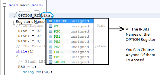
As y'all tin can see, they've created chip-fields of each register @ the same memory address in the RAM as in the datasheet. The fields' width is specified to be 1-Bit for each field, using this operator [:1 ] for each field. The fields' names are usually the same every bit in the datasheet.
Typically a scrap-fields for a specific register follows the convention shown below.
Xbits
Where Ten is the proper noun of whatever specific annals equally found in the datasheet. Which means that accessing whatever bit is easily done past writing the following.
Xbits.
This will list down all the bits of this register (fields) for you to choose from. Attempt it yourself!
Detect: In fact, other than pic16f877a.h file, there are many other header files that contain register maps and scrap-fields pre-divers and pre-written for all PIC microcontrollers inside the XC8. Which is a gratuitous open up-source lawmaking that you should definitely take advantage of.
ii. Read/Write digital i/o pins
Later on configuring any i/o pin, y'all'll be able to read its state (if it's an input pin) or to change its logical land (if information technology'south an output pin). Here the role of PORTx register comes in, equally the value we write to that register specifies the logical state of the corresponding pins (High 1/ Low 0).
- Writing 1 (Loftier) to a single chip of the PORTx register sets the respective pin to be High.
- Writing 0 (Depression) to a single bit of the PORTx register sets the corresponding pivot to be Depression.
Which means that writing the following values to these bits will bring us the following results
| Value | Bit | Upshot |
| 1 | RB2 | RB2 pin is driven High (logic 1), merely it must kickoff exist configured as an output pin |
| 0 | RB3 | RB3 pin is driven Low (logic 0), simply it must first exist configured as an output pin |
| i | RC5 | RC5 pivot is driven High (logic 1), but information technology must first be configured as an output pin |
| 0 | RD7 | RD7 pin is driven Low (logic 0), merely it must first exist configured as an output pin |
| Then on… | ||
ane. Reading digital Inputs
Reading-in the logical state of an input pin requires additional hardware connections in order to guarantee a stable system behavior. A typical pin can be driven to Loftier, Depression or left Floating. Still, you lot shouldn't go out whatsoever i/o pin floating in the air as long as you're using it as an input for your arrangement.
The floating country must be avoided under any circumstances, every bit it'due south not deterministic consistent input. It totally depends on how noisy the environment is. For this reason, input pins are generally pulled-down or pulled-up.
- Input Pins Pull-Up
In this configuration, the pin is e'er pulled-up to Loftier (logic 1) until an event occurs to bulldoze information technology Low (to 0). By and large all you need to have is a 10kohm resistor connected between the input pin and the Vdd (+5v) as shown below.
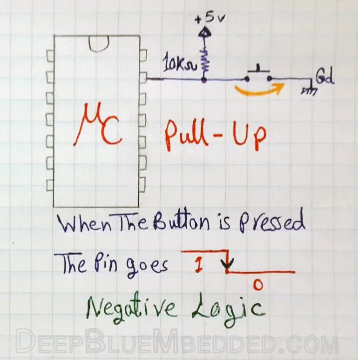
The logical country of the pin is always 1 until the push button is pressed, then information technology'south short-circuited with basis and becomes 0. This is called Negative Logic input, equally the action of the user (pressing button) transfers the digital pin land from High to Depression.
- Input Pins Pull-Downward
In this configuration, the pivot is always pulled-downwardly to Low (logic 0) until an upshot occurs to bulldoze it Loftier (to 1). Mostly all you demand to have is a 10kohm resistor connected betwixt the input pin and the Vss (0v or Gd) as shown below.
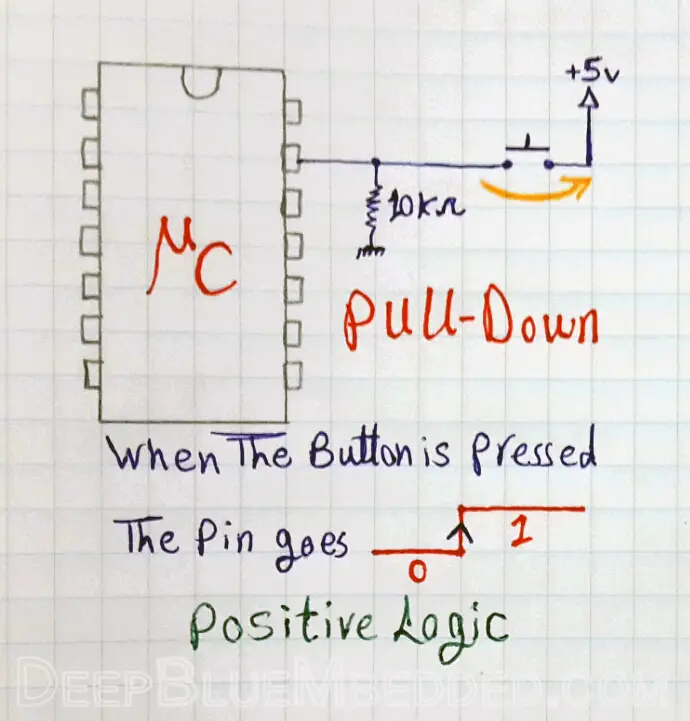
The logical state of the pivot is always 0 until the button is pressed, then information technology's short-circuited with Vdd (+5v) and becomes i. This is called Positive Logic input, as the action of the user (pressing button) transfers the digital pin state from Low to Loftier.
| Note | |||
| Some pins have internal Pull-Upwardly resistors built-in the microcontroller itself (e.yard. PORTB pins). However, in near cases, you'll have to cull & create one of the 2 configurations in a higher place which are identical in function but reversed in logic handling mechanisms. | |||
Let's take a simple example for reading a digital input. Say we've got an i/o pivot called RD4 which is configured to exist an input pin. This pin is connected to a Pull-Down resistor with a small-scale button button. Nosotros're willing to do something when the user presses the button. The C-Lawmaking for this is shown below.
| if ( PORTDbits . RD4 == 1 ) { // Practice something ... } |
or equivalently
| if ( RD4 == ane ) { // Do something ... } |
or equivalently
| if ( RD4 ) { // Do something ... } |
Take the time to become familiar with these concepts and play effectually to make sure that everything you understand is really behaving as it should be.
| Hint | |||
| Checking the input pins' states using command flow logic (east.g. if, else, switch, while, etc.) is called Polling and it'south not the best choice for treatment critical input signals to the organization specifically those which crave an instantaneous response from the system (Existent-Time). This volition be discussed subsequently in The Interrupts Tutorial. | |||
For now, we're done with reading digital inputs and let'south move on to run across how we can write to the digital output pins in our microcontroller.
2. Writing Digital Outputs
Writing to the PORTx register will change the logical state of i/o pins (merely if they are configured as output pins). The output pins' logical states 0, 1 corresponds to 0v, +5v respectively. Which means that a typical output pin could possibly be sourcing electric current to other devices or it could be sinking current instead.
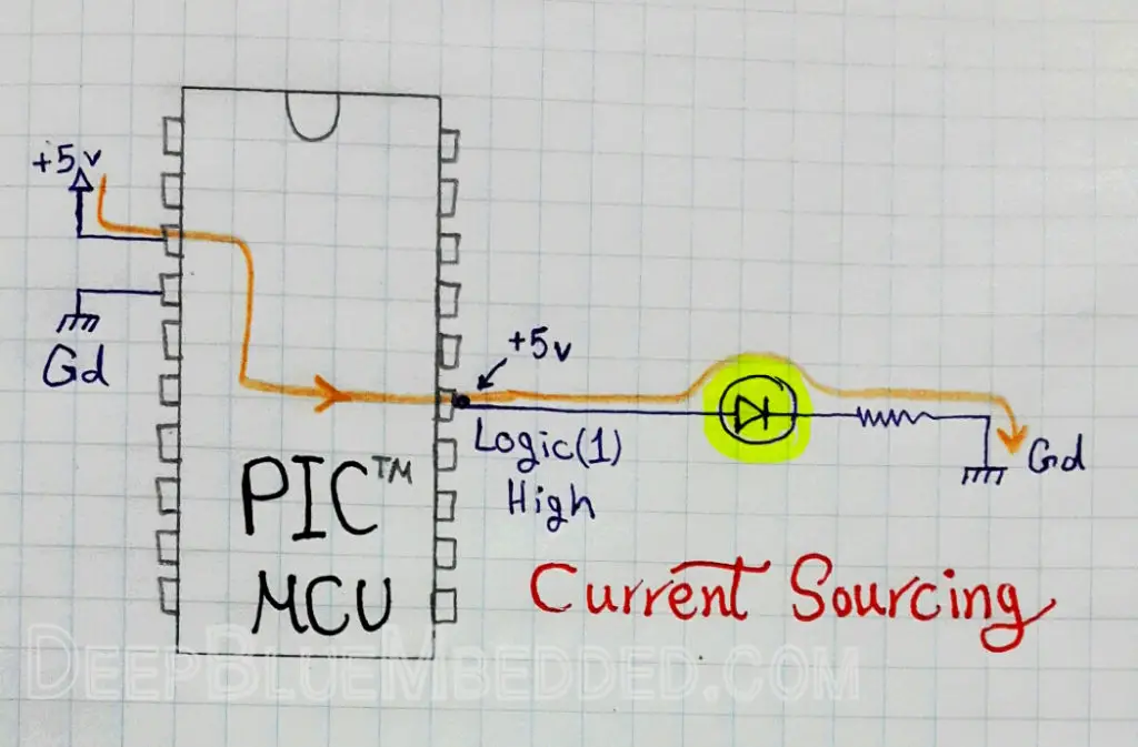
- Output Pins Current Sourcing
In this configuration, the output pin is used as a (+5v) source that delivers current to bulldoze very pocket-size loads (due east.g. LEDs, Transistors, Relays, Optocouplers, etc.). A typical pivot in our microcontroller can source up to 25 mA for each i/o pin and this value varies from an MCU scrap to another. This is the well-nigh commonly used configuration and it should be clear in the diagram below.
- Output Pins Current Sinking
In this configuration, the output pivot is used as a (0v or Basis) that sinks electric current from small loads (e.m. LEDs, Transistors, Relays, Optocouplers, etc.). A typical pin in our microcontroller can sink up to 25 mA for each i/o pin. This configuration is shown in the diagram below.
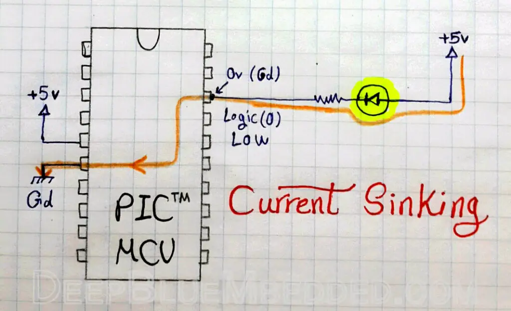
Check the datasheet for PIC16F877A, chapter 17.0 (Electrical Characteristics), page 173

| Note | |||
| You lot should never exceed the electric current limit for i/o pins at whatever cost. Otherwise, it'll cost you the entire scrap itself or at least some pins if y'all're lucky enough. Loads like DC motors, Stepper motors, Large LEDs assortment, etc. all of them could exist easily interface with a modest transistor biasing excursion. Y'all'll be safe and and then practice your MCU also. | |||
Permit's take a simple instance for writing a digital output. Say we've got an i/o pivot called RC5 which is configured to be an output pin. This pivot is connected to a 330 resistor with a small LED. We're willing to plough information technology on for i 2nd and turn information technology back off once more (Flash!). The C-Code for this is shown below.
| RC5 = 1 ; // Plow ON __delay_ms ( 1000 ) ; // Wait 1000ms = 1 2d RC5 = 0 ; // Plough OFF |
And at present we're done with the demo part of this tutorial and let'south motility on to the applied LABs.
Flashing some LEDs – LAB
| Lab Name | Flashing LEDs (Digital Output) |
| Lab Number | 1 |
| Lab Level | Beginner |
| Lab Objectives | Learn how to utilize GPIO pins for generating a digital output betoken and utilize it for flashing some LEDs. |
| Notation | |||
| All the LABs in this course are performed in 3 successive steps: 1- Coding 2- Simulation 3- Prototyping | |||
1. Coding
Open the MPLAB IDE and create a new projection name it "Flashing LEDs". If you take some issues doing then, you tin can always refer to the previous tutorial using the link below.

Gear up the configuration bits to match the generic setting which nosotros've stated earlier. And if yous besides find troubles creating this file, yous tin always refer to the previous tutorial using the link below.

At present, open the main.c file and allow'due south start developing the firmware for our project.
| Tip | |||
| Never forget to include the configurations header file within the master.c file of your projection. | |||
First of all, we've got three LEDs which will be hooked to 3 of our GPIO pins at PORTB. This means that we'll have to ready the data direction for 3 of the PORTB pins to be output pins. Let's use the following pins for our LAB [RB0, RB1, and RB2].
Setting the direction (input or output) of these pins is achieved via the TRISB register as follows.
| TRISB0 = 0 ; TRISB1 = 0 ; TRISB2 = 0 ; |
Afterward configuring the GPIO pins which we'll be using, information technology'due south fourth dimension to move to our main loop. In which we'll wink the LEDs in order. Each of them will exist ON for 50ms and OFF for another 50ms.
| one two 3 four 5 6 7 8 9 10 eleven 12 xiii 14 fifteen 16 17 eighteen | while ( 1 ) { // Flash LED1 RB0 = ane ; __delay_ms ( fifty ) ; RB0 = 0 ; __delay_ms ( 50 ) ; // Flash LED2 RB1 = 1 ; __delay_ms ( l ) ; RB1 = 0 ; __delay_ms ( 50 ) ; // Wink LED3 RB2 = one ; __delay_ms ( 50 ) ; RB2 = 0 ; __delay_ms ( fifty ) ; } |
| Note | |||||
| Using the __delay_ms() macro requires that the pre-defined name _XTAL_FREQ to be holding your actual oscillator's frequency value. For our example, we're using a 4MHz Crystal Oscillator. Which means that you must include the post-obit LOC at the beginning of your code.
| |||||
Cross your fingers. Hit the compile push! And we're done with the firmware.
2. Simulation
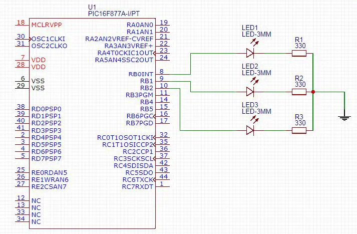
The schematic for this LAB is shown below. Just create a like ane in your simulator.
After connecting everything up in your simulator, you'll have to double-click the MCU bit and bespeak to the firmware code .hex file. The path volition be every bit follows
ProjectName.X > dist > default > production > FirmwareFile .hex
Make certain to simulate your project at the aforementioned oscillator frequency used in the code. Otherwise, the timing diagram will be messed-upward. Which means that the 50ms time delays in the code, will Not be a 50ms fourth dimension delay in the simulation if yous gear up OSC freq. to a value other than 4MHz!
| Note | |||
| While using some simulators, y'all won't be in need to connect the power supply 5v, crystal oscillator nor the pull-up resistor for the MCLR pin on your own. Which is the example for those who are using Proteus ISIS software. Still, any existent-life misconnection for whatever of these three will bring you lot into a real nightmare! There is so little chance of discovering that your Chip is insanely restarting all the time due to a dodgy MCLR pin or non being clocked at all due to OSC issues, so please, exist careful. | |||
3. Prototyping
Yous should have created the bones prototyping setup which we've prepared previously. If you've any troubles doing and then, you can refer to that previous tutorial.
Connect the RB0, RB1 and RB2 pins to the 1st, 2nd and 3rd LEDs Cathode leads. And then claw three resistors 330 betwixt the LEDs' anodes and the Footing line.
Plug the power supply et voila! you've accomplished your first (Hello World) embedded projection. Congratulations!
The final running project in instance you're curious.
 |
Reading Digital Inputs – LAB
| Lab Name | Reading Digital Inputs (Digital Input) |
| Lab Number | two |
| Lab Level | Beginner |
| Lab Objectives | Learn how to utilize GPIO pins for reading a digital input indicate and using information technology to command the flashing of an LED. |
1. Coding
Open the MPLAB IDE and create a new project proper noun information technology "Digital Input". If yous take some issues doing so, you can e'er refer to the previous tutorial using the link beneath.
Set the configuration bits to match the generic setting which we've stated earlier. And if y'all as well discover troubles creating this file, you can always refer to the previous tutorial using the link below.
Now, open the main.c file and let's beginning developing the firmware for our project.
We'll use a couple of GPIO pins:
- The first one will operate as a digital input pin and will exist hooked to the push button to read its logical state (high/depression).
- The 2d pin volition operate equally a digital output pin and will be hooked to the LED in club to wink it twice per second.
Let'southward set the RB0 pin to be an input pin and RB1 to exist an output. To configure these pins we'll write the following lawmaking.
| TRISB0 = ane ;// Input Pin TRISB1 = 0 ;// Output Pin |
Afterward configuring the GPIO pins which nosotros'll be using, it's time to move to our master loop. In which we'll read the country of the button hooked to pinRB0. And if information technology's pressed down, we'll flash the LED hooked toRB1 pivot.
| while ( 1 ) { if ( RB0 == 1 ) { // If the push button is pressed, flash the LED twice/2d. RB1 = 1 ; __delay_ms ( 250 ) ; RB1 = 0 ; __delay_ms ( 250 ) ; } } |
| Note | |||||
| The fleck-fields could be treated as if they are boolean variables. Which means that the RB0 checking (polling) could accept been washed with the post-obit LOC without equality check (==i).
| |||||
Cross your fingers. Hit the compile button! And we're done with the firmware.
ii. Simulation
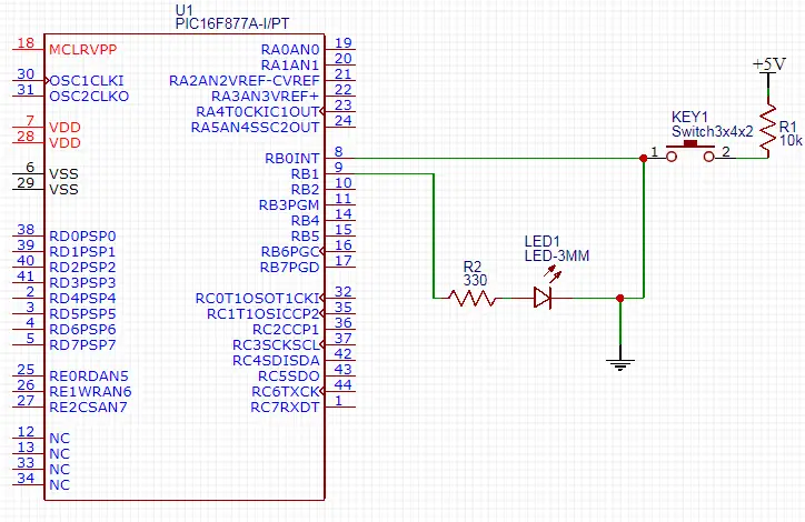
The schematic for this LAB is shown beneath. Merely create a similar ane in your simulator.
Later on connecting everything up in your simulator, you lot'll have to double-click the MCU bit and betoken to the firmware code .hex file, make sure to simulate your project at the same oscillator frequency used in the lawmaking. Otherwise, the timing diagram volition be messed-upwardly.
iii. Prototyping
Yous should have created the basic prototyping setup which we've demonstrated previously. If y'all've whatsoever troubles doing and then, you can refer to that previous tutorial.
Connect the RB0 pin to the push which is connected in pull-downwardly way. Connect the RB1 pin to the LED's cathode. Then hook resistors 330 betwixt the LED's anode and the Ground line.
Plug the power supply and test this out!
The concluding running project in case you're curious.
| |
The ability of #define directive
When you're dealing with Input/Output post, whatever platform is existence used, information technology becomes fundamentally much more efficient to use the pre-processor #defineinstead of writing directly to bits or registers. Let's consider the following LOC for example.
What this directive actually does is telling the compiler earlier assembling code to replace every single occurrence of LED1in your lawmaking with RB0.Which means that y'all can switch the LED hooked to RB0 pin ON and OFF in the following manner.
| LED1 = 1 ; // ON LED1 = 0 ; // OFF |
This practice is highly recommended not but for debugging purposes but also for portability, readability and the like. It's ultimately the all-time style to deal with i/o ports, and it's also substantial for creating libraries that are easily portable. Let's take just 1 concrete example to see the real power of the and then-called#ascertain pre-processor. Consider the following code
| while ( i ) { RC1 = 1 ; __delay_ms ( 100 ) ; RC1 = 0 ; __delay_ms ( 100 ) ; RC1 = 1 ; __delay_ms ( 200 ) ; RC1 = 0 ; __delay_ms ( 200 ) ; RC1 = ane ; __delay_ms ( 300 ) ; RC1 = 0 ; __delay_ms ( 300 ) ; } |
This lawmaking evidently toggling the logical state of the RC1 pin for 100ms, 200ms, and 300ms. Well, allow's suppose for whatever reason you lot're forced to get out the RC1 pin and move the (e.g. LED) and hook it to another i/o pivot. Let'southward say you'll motion information technology to RD1 pin. At present, yous'll go to the code and make some modifications at every occurrence for RC1 to replace it with RD1. Which is obviously an unnecessary additional overhead, and the final results will never be consistent nor efficient. Yet, allow's do those modifications.
| while ( 1 ) { RD1 = ane ; // Showtime line needed modification __delay_ms ( 100 ) ; RD1 = 0 ; // 2d __delay_ms ( 100 ) ; RD1 = ane ; // 3rd __delay_ms ( 200 ) ; RD1 = 0 ; // 4 __delay_ms ( 200 ) ; RD1 = 1 ; // 5 __delay_ms ( 300 ) ; RD1 = 0 ; // 6 __delay_ms ( 300 ) ; } |
The determination of moving an i/o pin has resulted in roughly 6 lines that needed correction. It'due south not always the example of class and you may be in a situation in which this issue could leave you with a couple of hundreds LOC waiting to be corrected! Just consider instead if you lot're using the #define in the following fashion.
| 1 two 3 iv 5 half dozen 7 viii 9 10 11 12 13 14 15 16 17 | #define LED1 RC1 . . while ( ane ) { LED1 = 1 ; __delay_ms ( 100 ) ; LED1 = 0 ; __delay_ms ( 100 ) ; LED1 = ane ; __delay_ms ( 200 ) ; LED1 = 0 ; __delay_ms ( 200 ) ; LED1 = 1 ; __delay_ms ( 300 ) ; LED1 = 0 ; __delay_ms ( 300 ) ; } |
This code is typically the exact same equivalent of the first example. Which toggles the RC1 pin for varying time intervals. However, when a change has to be made for the i/o pin nosotros are using, and allow's say we're migrating the LED from RC1 to the RD1 pin. The ONLY alter that must exist made is just the first LOC as follows.
| Pro Tip | |||
| E'er pick relevant names for the #define pre-processor. Cypher is more painful than irrelevant naming for i/o, variables, functions or any. So please, pay attending and invest a couple of seconds of your time thinking near a relevant name that exactly describes your identifier. | |||
Checkout My PIC MCU Programming Video Tutorial
| Picture Microcontrollers Form Home Page 🏠 | |||||||
| | Previous Tutorial | Tutorial 4 | Side by side Tutorial | | |||

Are There Any Downsides To Using One Register For All I/o In Pic,
Source: https://deepbluembedded.com/input-output-io-ports-gpio-pins/
Posted by: mcgeewhisen.blogspot.com
0 Response to "Are There Any Downsides To Using One Register For All I/o In Pic"
Post a Comment